NCP1927
http://onsemi.com
5
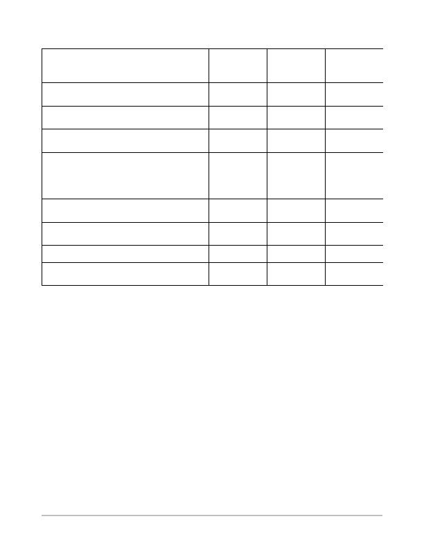
MAXIMUM RATINGS (Note 1)
Rating
Symbol
Value
Unit
Supply Pin (pin 13) (Note 2)
Voltage Range
Current Range
V
CC(MAX)
I
CC(MAX)
0.3 to 30
$30
V
mA
PFC Drive Pin (pin 14) (Note 2)
Voltage Range
Current Range
V
PDRV(MAX)
I
PDRV(MAX)
0.3 to 20
800, +1200
V
mA
Flyback Drive Pin (pin 12) (Note 2)
Voltage Range
Current Range
V
FDRV(MAX)
I
FDRV(MAX)
0.3 to 20
800, +1200
V
mA
Inverter Enable Pin (pin 16) (Note 2)
Voltage Range
Current Range
V
IENABLE(MAX)
I
IENABLE(MAX)
0.3 to 6
$20
V
mA
Control Pin (pin 4) (Note 2)
Voltage Range
Current Range
V
PControl(MAX)
I
PControl(MAX)
0.3 to 6
$10
V
mA
PFC Current Sense Pin (pin 7) (Note 2)
Voltage Range
Current Range
V
PCS(MAX)
I
PCS(MAX)
0.3 to 3
$10
V
mA
ZCD Pin (pin 6) (Note 2)
Voltage Range
Current Range
V
PZCD(MAX)
I
PZCD(MAX)
0.9 to 12
$10
V
mA
All Other Pins (Note 2)
Voltage Range
Current Range
V
MAX
I
MAX
0.3 to 10
$10
V
mA
Thermal Resistance
JunctiontoAir, 100 mm
2
Single Layer of 1 oz Copper
R
窲A
140
癈/W
Temperature Range
Storage Temperature
Operating Junction Temperature
T
JSTRG(MAX)
T
J(MAX)
60 to 150
25 to 125
癈
Stresses exceeding Maximum Ratings may damage the device. Maximum Ratings are stress ratings only. Functional operation above the
Recommended Operating Conditions is not implied. Extended exposure to stresses above the Recommended Operating Conditions may affect
device reliability.
1. This device series contains ESD protection and exceeds the following tests:
Charged Device Model 2000 V per JEDEC Standard JESD22-C101D
Human Body Model 2000 V per JEDEC Standard JESD22A114E
Machine Model 200 V per JEDEC Standard JESD22A115A
2. This device contains latchup protection and exceeds 100 mA per JEDEC Standard JESD78.
发布紧急采购,3分钟左右您将得到回复。
相关PDF资料
NCP380HMU21AATBG
IC CURRENT LIMIT SWITCH 6-UDFN
NCT1008DMT3R2G
TMP DIO MON/SMBUS 4CH 8WDFN
NCT210RQR2G
IC TEMP SENSOR LOC/REM 16QSOP
NCT214MT3R2G
IC TEMP SENSOR LOC/REM 10WDFN
NCT72CMNR2G
IC REMOTE THERMAL SENSOR 8-DFN
NCT7491RQR2G
IC REMOTE THERMAL MONITOR 24QSOP
NCT75MNR2G
IC SENSOR TEMP DGTL 8DFN
NCV8881PWR2G
IC REG TRPL BUCK/LINEAR 16SOIC
相关代理商/技术参数
NCP1937A1DR2G
制造商:ON Semiconductor 功能描述:COMBO PFC & QUAZI FLYBACK - Tape and Reel 制造商:ON Semiconductor 功能描述:REEL / COMBO PFC & QUAZI FLYBACK
NCP1937B1DR2G
制造商:ON Semiconductor 功能描述:COMBO PFC & QUAZI FLYBACK - Tape and Reel
NCP1937BADAPGEVB
制造商:ON Semiconductor 功能描述:ADPTR 90W PFC+QR<10MW - Bulk 制造商:ON Semiconductor 功能描述:BOARD EVAL FOR NCP1937 制造商:ON Semiconductor 功能描述:Power Management IC Development Tools 90 W Adapter PFC+QR 10 MW Eval Brd
NCP21WB333
制造商:MURATA 制造商全称:Murata Manufacturing Co., Ltd. 功能描述:for Surface Mounting Application
NCP21WB333J03RA
功能描述:热敏电阻 - NTC 33K OHM 5%
RoHS:否 制造商:EPCOS 电阻:10 kOhms 功率额定值:150 mW 容差:2 % 端接类型:Radial 系列:B57703M 工作温度范围:- 55 C to + 125 C
NCP21WB333K03RA
功能描述:热敏电阻 - NTC 33K OHM 10%
RoHS:否 制造商:EPCOS 电阻:10 kOhms 功率额定值:150 mW 容差:2 % 端接类型:Radial 系列:B57703M 工作温度范围:- 55 C to + 125 C
NCP21WB473
制造商:MURATA 制造商全称:Murata Manufacturing Co., Ltd. 功能描述:for Surface Mounting Application
NCP21WB473J03RA
功能描述:热敏电阻 - NTC 47K OHM 5%
RoHS:否 制造商:EPCOS 电阻:10 kOhms 功率额定值:150 mW 容差:2 % 端接类型:Radial 系列:B57703M 工作温度范围:- 55 C to + 125 C
